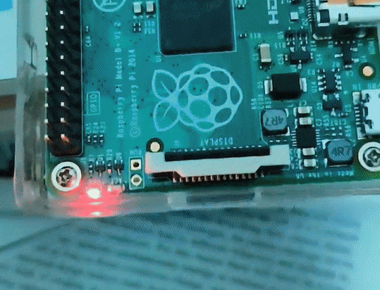
Controlling the ACT LED on RPi B+
10 Jun 2022 | programming, os, rpi, side-projectThe RPi boards generally have two LEDs on board. The first, PWR LED represents the power in the board and the second ACT LED can be programmatically controlled. The ACT LED is easy to control and can be used as a good indicator that my code running on the RPi until I can get complex output functions to get working.
There is an excellent Baking Pi course which focuses on bare programming on RPi in assembly. It targets the RPi 1 B model. I tried following the OK01 tutorial but couldn’t get it to work on my B+ model, no matter how hard I tried. And as I was about to give up, I chanced upon a very nice blog written by Glenn Lockwood and with its help I was finally able to make the led glow.
Although the blog by Glenn gives a very nice explanation about the details of how the code works, my post adds a bit more information regarding where that information can be found in official sources to enable the reader to explore more.
Major changes from RPi B to RPi B+
There are two significant changes regarding the behavior of ACT LED between the 2 models:
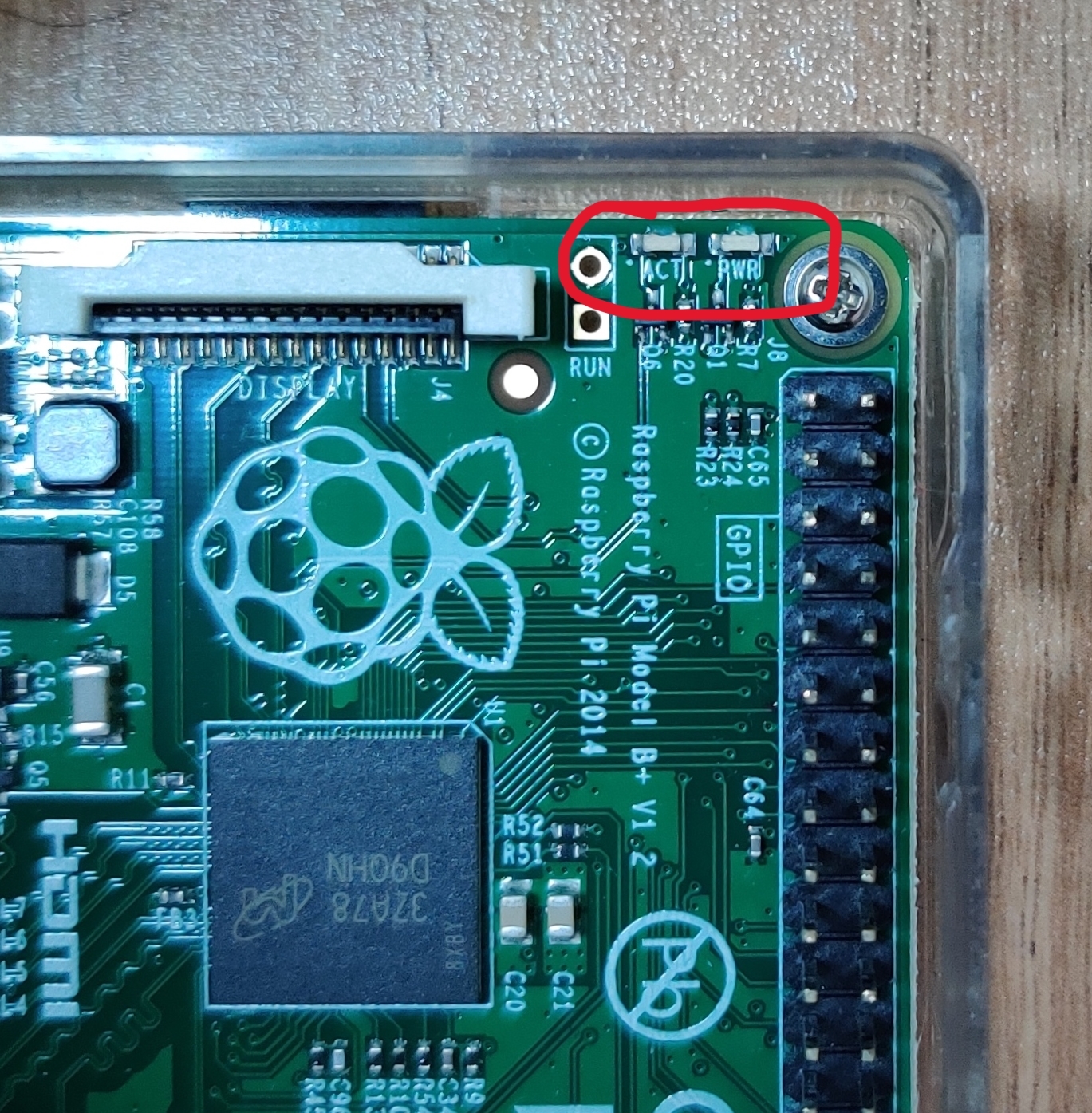
- The ACT LED was connected to GPIO pin 16 on RPi B, but starting RPi B+ and all newer models it is connected to pin 47.
- Earlier to make the LED glow we had to set the GPIO pin to off (yes we had to set it off) while in the newer model we set it to 1 to make the led glow.
I couldn’t find any of this information from the official source. Even the schematics available on RPi’s website don’t talk about ACT LED. The only information I could find was through this discussion forum.
Enabling the LED
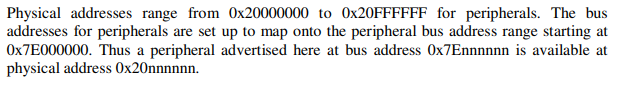
Now we know that the ACT LED is connected to GPIO pin 47 of the SoC in RPi, and enabling it will make the LED glow. The RPi B+ model uses the Broadcom BCM2835 SoC. Let’s head over to the BCM2835 manual. We can easily spot the chapter that is relevant for our purpose: “6 General Purpose I/O (GPIO)”. But before heading there we need to find the memory mapping used by the SoC. The BCM2835 has a two layer address translation. First the virtual address used by the ARM core is translated to physical address by the ARM MMU and then the physical address are once again translated by the VC MMU to bus address which finally maps to the RAM or the peripheral devices.

For our example we won’t be enabling the ARM MMU and will be using physical addresses direclty in our code. The peripheral addresses specified in the manual are all bus address so we need to find the mapping between physical and bus address. It is available in section 1.2.3.
Now let’s head over to chapter 6. Manipulating a GPIO pin involves 2 steps.
- First we need to set the GPIO pin 47 in the output mode using
GPFSELregister - Then we need to the set the bit corresponding to GPIO pin 47 in
GPSETregister as 1
The address of the register can be seen in the following table:
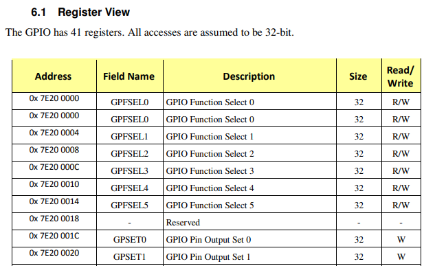
GPFSEL
Each GPIO can do multiple functions based on the 3 bit value set in GPFSEL register. Each register has 32bits and hence can store the
data for 10 registers. For a total of 54 GPIO pins we have 6 GPFSEL registers. The register of interest for us is GPFSEL4 (the
register names are 0 indexed):
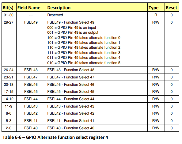
To set a GPIO pin as output pin we need to set FSEL47 to 001 which means we need to write the following value in GPFSEL4
register:

In order to make the code easier to understand we will always use relative address from the base GPIO address (0x20200000). The GPFSEL4
is 0x20200010 - 0x20200000 = 16 bytes away from the base address.
Remember that addresses are always byte-addressed meaning an address indicates the address of 8-bit/1-byte of data and the next address will point to the next byte of data.
The below code shows how to set the value:
ldr r0,=0x20200000  // set the base address
mov r1,#1
lsl r1,#21          // shift the 1 by 21 places
str r1,[r0,#16]     // store the value at base address + 16
GPSET
We have the GPIO pin 47 as output pin but now we need to actually set the output of the pin as 1. For this we will use the GPSET
register. In the GPSET register each bit represents the output of the GPIO pin. There are 2 registers to represent the output of 54
GPIO pins. To set the output of pin 47 we need to update the GPSET1 register.
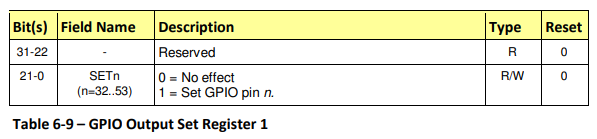
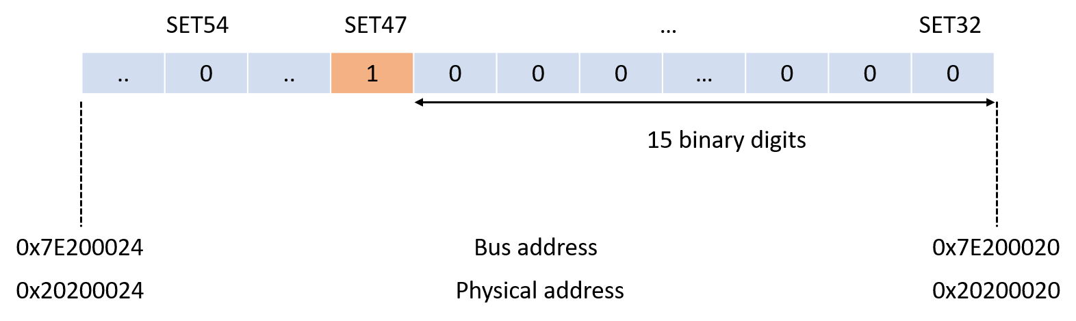
We will write the following value in the register:
The below code shows how to set the value:
mov r1,#1
lsl r1,#15          // shift the 1 by 15 places
str r1,[r0,#32]     // store the value at base address + 32
Final Code
.section .init
.globl _start
_start:

ldr r0,=0x20200000  // set the base address
mov r1,#1
lsl r1,#21          // shift the 1 by 21 places
str r1,[r0,#16]     // store the value at base address + 16

mov r1,#1
lsl r1,#15          // shift the 1 by 15 places
str r1,[r0,#32]     // store the value at base address + 32

loop$:
b loop$
Refer to the OK01 lecture of the Baking Pi series for the Makefile and linker scripts. It also shows how to get the code running on the real hardware.